
 中文简体
中文简体

ABSTRACT
Designing micro-optics for light-emitting diodes must take into account the near-field radiance and relative spectral power distributions of the emitting LED die surfaces. We present the design and application of a near-field goniospectroradiometer for this purpose.
Keywords: Near-field photometry, goniophotometer, LED measurement, spectroradiometer
1. INTRODUCTION
One of the often-touted advantages of high-flux light-emitting diodes (LEDs) is that they are “point sources” of light, which in theory greatly simplifies the design of non-imaging optical systems such as architectural light fixtures (or “luminaries”) and LED backlight systems.
The situation in practice is more complex. It is often necessary to employ arrays of LEDs in order to compete with traditional incandescent and fluorescent light sources. The size and density of the array is usually limited by LED thermal considerations – LEDs generate considerable amounts of heat – and so the aggregate light source can no longer be considered a “point source” for optical design purposes.
One solution to this problem is to couple each LED die to a micro-optical element with refractive and possibly diffractive microstructures. These elements can be mounted close to the LED die or molded directly onto the surface of its optical epoxy encapsulate. They can also be applied directly to the encapsulate surface using ultraviolet replication techniques.
In order to design efficient refractive and diffractive optical elements, we need to know the LED die geometry, including its size, shape, and position within its encapsulate. We also need to know the 2D radiance distribution across the surface of the emitting die surface and its relative spectral power distribution. It is not sufficient to model the LED die as a uniform Lambertian emitter, as the spatial distribution of radiance can, depending on the current spreading layer design and bond wire placement on the die, be highly non-uniform.
A useful technique for measuring these parameters can be developed from instrumentation that was originally developed for near-field photometry of architectural luminaries.
2. NEAR-FIELD PHOTOMETRY
Near-field photometry was first developed to measure and model the near-field luminous flux distribution of architectural luminaries. It uses a digital camera to measure the four-dimensional scalar field of light surrounding a volume light source such as a lamp or luminary. With these measurements, it is possible to accurately model the illuminance distribution over any surface, regardless of its distance, orientation or curvature with respect to the light source.
The key concept is the geometric ray of light. The IESNA Lighting Handbook defines illuminance E as “the luminous flux per unit area incident at a point on a surface.” That is, illuminance is due to light coming from all directions above a surface and intersecting a point, where the “surface” can be real or imaginary. We can think of this light as an infinite number of geometric rays coming from every direction above the surface plane, each with its own quantity of luminous flux.
If we can measure the luminance of each ray, we can calculate the illuminance at the point. A ray of light travels in a straight line through an optically homogeneous medium such as air. Because the quantity of luminous flux within the ray does not change (neglecting scattering and absorption), neither does its luminance. We can therefore measure the luminance of a ray anywhere along its length.
Now, consider a planar or volumetric light source surrounded by an imaginary sphere. Every ray of light emitted by the light source will have to intersect this sphere at some point. We can therefore think of the light source being surrounded by a four-dimensional scalar photic field, wherein each point has two position coordinates and two direction coordinates.
We can measure the luminance of a single ray of light with a lens-type luminance meter. More accurately, we can measure the average luminance of a bundle of rays contained within a cone defined by the photo sensor area, the lens aperture and focal length, and the focus point. In practical terms, this may still be considered representative of a single ray for a luminance meter with a sufficiently narrow field of view. (The “surface” that the luminance meter is focused on can be real or imaginary.)
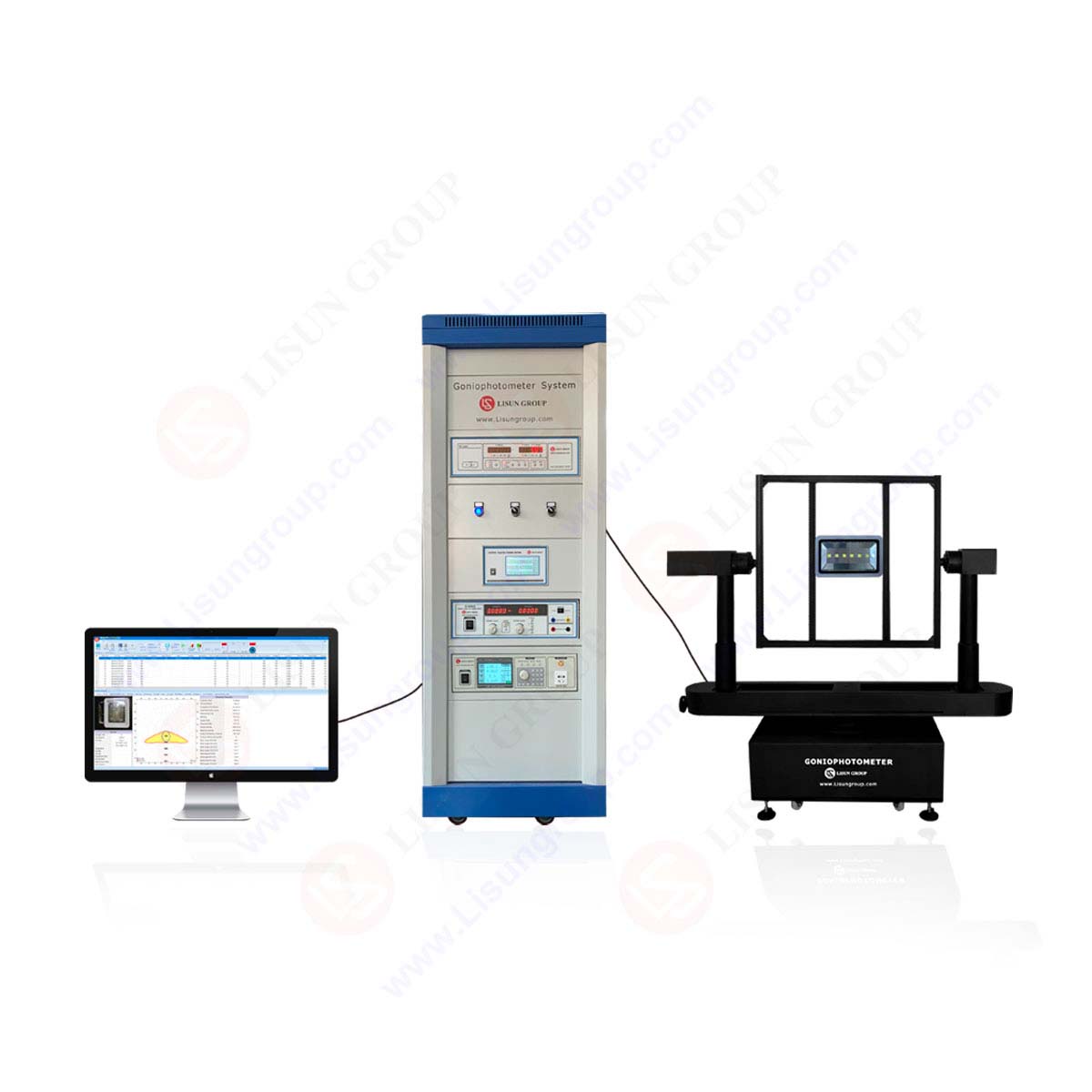
For the purpose of a practical near-field goniophotometer (product list of goniophotometer), we can replace the lens-type luminance meter with a photometrically-or radiometrically-calibrated digital camera, wherein each image pixel measures the luminance or radiance of a unique geometric ray. With an image resolution of (say) 1024 × 1024 pixels, a digital camera can simultaneously measure the luminance of over one million rays that converge on the camera lens.
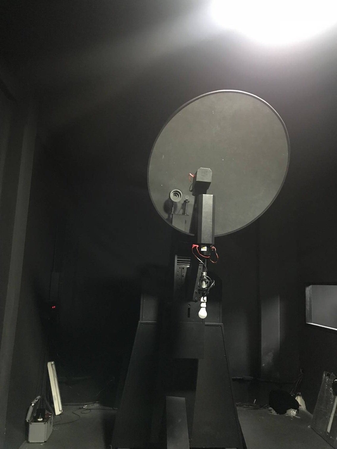
If we mount the camera on a moveable arm that rotates in the vertical plane about the light source and rotate the light source in the horizontal plane, the camera will circumscribe an imaginary sphere about the light source. By capturing images at closely spaced intervals in the vertical and horizontal planes, we can thus adequately sample the surrounding photic field. The luminance of an arbitrary geometric ray can then be interpolated from this set of measured rays.
Practical near-field goniophotometers have been constructed. For example, Ashdown used the resultant ray set to predict the luminance distribution of architectural surfaces near linear fluorescent luminaries, while Rykowski characterized incandescent and high-intensity discharge lamps for non-imaging optical design using ray-tracing techniques. Other examples include near-field goniophotometers designed and constructed for high-intensity discharge lamps, automotive headlights, and computer graphics applications.
3. NEAR-FIELD GONIOSPECTRORADIOMETER DESIGN
Like most laboratory instruments, that is truly innovative in the design of a near-field goniophotometer. Rather, the devil is in the details. Designing and constructing an instrument specifically for LED light measurement includes a number of issues that must to be considered for a successful implementation.
3.1 Spectral Power Distribution
Most traditional light sources, including incandescent, fluorescent, and high-intensity discharge lamps, exhibit essentially constant relative spectral power distributions under normal operating conditions and so goniophotometric measurements (both near-field and far-field) are typically performed with photopically-corrected broadband photosensors.
High-flux LEDs differ in that their peak emission wavelengths vary with LED die junction temperature, typically 0.04nm/℃ for InGaN (blue and green) LEDs and 0.6 to 0.9 nm/℃ for AlInGaP (red and amber) LEDs. In addition, their approximately Gaussian spectral power distributions (ignoring phosphor-coated white light LEDs) exhibit spectral broadening with increasing junction temperature, for AlInGaP LEDs, where is in nm and T is in Kelvin. The spectral power distributions and spectral broadening characteristics of InGaN LEDs are more complicated, but have been recently been successfully modeled. These are not academic issues, as high flux LEDs are inherently dimmable, and so they may be expected to operate with junction to as much as185℃ at full power. Changes in peak wavelength and spectral bandwidth affect both the chromaticity and luminous intensity of LEDs.
Phosphor-coated LEDs represent another challenge. In addition to the temperature-dependent spectral characteristics of the blue InGaN LED used to optically pump the phosphors, the phosphors themselves may exhibit temperature dependencies. Worse, the phosphor coating may have an uneven thickness, which can result in LED chromaticity variations with viewing angle.
It is a reasonable assumption that the emission spectrum of a semiconductor die will remain approximately constant across its emitting surface. However, given that the spectrum may be both temperature and spatially dependent, it should be monitored and recorded during image acquisition. This can be accomplished by placing a beam-splitter between the camera lens and image sensor, with a portion of the light directed to a fiber optic-coupled spectroradiometer (fiber optic spectrometer). A relative spectral power distribution can then be captured with each image and later used to generate a hyper spectral ray set for non-imaging optical design, or at least apply necessary corrections for ray luminance calculations.
Another reason for using a spectroradiometer instead of a photopically-corrected broadband photosensor – and this applies to all LED luminous flux measurements – is that broadband sensors with photopic filters often exhibit unacceptably large errors when measuring light luminous flux from narrowband blue sources. The spectroradiometer measurements can be used to calibrate the digital camera’s spectral response and thereby obtain accurate luminance or radiance values for the measured geometric rays.
3.2 Imaging Optics
Another issue of concern is the camera lens. Rea provides a good overview of the issues concerning vignette compensation and focus, but the small size of LED die means that diffraction and depth of field also become issues. A close-up view of the epoxy-encapsulated LED die with its gold bond wire. The camera lens was stopped down in order to maintain an adequate depth of field but only at the expense of diffraction-limited resolution.
The tradeoff between resolution and depth of field is dependent on the size of the LED die and the need for precision in the interpolated ray set when designing non-imaging optics. For most applications, the resolution indicated by is likely adequate, as there is considerable variation in the placement of the bond wires with commercial LEDs. Regardless, any non-imaging optical design should take into account LED (LED test) manufacturing tolerances.
An interesting solution to this problem that we are currently investigating is the recently introduced plenoptic camera. Coaxially interposing a lenticular micro lens array between the primary objective and the image sensor produces an array of low resolution images that effectively sample the four-dimensional photic field with a single exposure. Image analysis techniques can then be employed to resort the rays where they would have terminated in a virtual camera at a slightly different position. As a result, the depth of field and focus of the camera can be adjusted a posteriori without reducing the camera aperture or increasing the exposure time.
3.3 Image Sensor
LED die is grossly overexposed. This is due to the 8-bit dynamic range of the file format used for the illustration. In practice, a minimum of 12 bits dynamic range is usually required for image capture and analysis. This can be achieved with a cooled scientific-grade CCD camera (CCD spectrometer) or with a CMOS camera using different exposures and high-dynamic range imaging techniques. Multiple images can also be captured and averaged to reduce thermal noise, while a dark frame image can be captured and subtracted from the averaged images to compensate for per-pixel bias and “hot” pixels.
Most digital cameras exhibit a nonlinear response to incident radiant flux over their dynamic range. Fortunately, a simple radiometric self-calibration technique can be employed to measure and thereby linearize the camera-lens response.
3.4 Data Compression
There are also data representation issues to consider. The problem is that a data set of raw 12-bit images may require gigabytes of disk space. Ashdown presented a simple lossless algorithm using Haar wavelets to achieve 90 percent data compression that also offered extremely fast decompression for on-demand image retrieval when generating interpolated ray sets. Similar work has been done in other fields, including light field rendering in computer graphics and MRI scanner data sets in medicine.
Data compression is not an important issue per se with respect to the design of a near-field goniospectroradiometer, but it is necessary in order to implement a practical instrument. Ideally the compressed image data file is sufficiently small that it is practical for LED (LED testing) manufacturers to provide the data to their customers on DVD-ROM or via the Internet.
3.5 Camera Positioning
As will be understood from the following section on data interpolation, it is convenient but not essential to have the digital camera positions evenly spaced on the imaginary sphere surrounding the light source. This can be accomplished by tiling the sphere with identically-sized equilateral triangles. (Tiling a hemisphere in this manner yields the familiar geodesic dome.) The advantage of this approach is that the ray luminance interpolation algorithm becomes independent of the camera position.
Calculating the exact camera positions in spherical coordinates is easily accomplished by recursively subdividing the triangular faces of an octahedron, where each subdivision quadruples the number of equilateral triangles. This technique is commonly used in computer graphics to mesh the surfaces of spherical and hemispherical objects. (It is so common that there is no proper name for the recursive algorithm. Paradoxically, it is only rarely discussed in computer graphics or computational geometry textbooks.)
Choosing the appropriate subdivision level depends on both the three-dimensional complexity of the light source’s photic field and the desired accuracy of the interpolated ray set. For most commercially available high-flux LEDs, three levels of subdivision (145 vertices and 256 triangles) are usually sufficient. However, if the LED (LED tester) die or package exhibits a narrow beam pattern due to collimating lenses or photonic crystals, four levels of subdivision (545 vertices and 1024 triangles) may be required.
3.6 Data Capture
Image and spectra capture follow the usual procedures for digital photometric measurements. The LED is energized and allowed to thermally stabilize, while a three-axis mechanical stage is used to precisely align the LED with respect to the goniometric center of rotation. An initial dark field image is then captured with the lens covered to record the per-pixel bias values due to thermal noise, following which the camera arm and LED mount are successively positioned to each vertex of the imaginary geodesic dome.
Multiple camera images are captured at each vertex position to reduce the signal-to-noise ratio while obtaining a highdynamic range composite image. Meanwhile, the LED spectrum is measured with the through-lens spectroradiometer, while the LED forward voltage is monitored to determine the die junction temperature.
Once the images and associated spectra have been captured and their data suitably compressed, they can be written to disk for later retrieval and data interpolation to generate ray sets.
3.7 Ray Interpolation
Many non-imaging optical design programs support the importation of ray sets based on physical measurements. These include position and direction information for each ray, and optionally wavelength for refractive and diffractive systems design.
Depending on the design requirements, a ray set may consist of several thousand to several million random rays. The advantage of archiving the images and associated spectra from the near-field goniospectroradiometer is that an optical engineer can generate a posteriori as many random rays as required, and also specify the desired range of positions and angles for a particular project.
Choosing the start position for a random ray can be based on the known geometry of the LED die and its mount. In the simplest case, the LED die can be assumed to be planar, and with a width delimited by the camera field of view when seen from directly above. Any ray whose interpolated luminance is less than a predetermined noise threshold can later be rejected from the ray set.
Geometric models of the LED die can also be used, although manufacturing tolerances for the bond wire placement may lead to significant uncertainties. If necessary, the three-dimensional geometry of the LED die can be derived using stereo disparity techniques as described in the computer vision literature.
4. CONCLUSIONS
Designing micro-optics for light-emitting diodes will present numerous engineering challenges. While current efforts have concentrated on optical designs for handheld devices such as backlit PDA and cellular phone displays, there are opportunities and challenges for backlit television displays and solid-state lighting as well.
The near-field goniospectroradiometer we have described in this paper provides detailed information on the near-field radiance and relative spectral power distributions of the emitting LED die surfaces. We have only recently completed its design and construction, and we are currently in the process of commissioning the instrument. We fully expect however that it will prove invaluable in our company efforts to develop next-generation optical components for solid-state lighting systems.
Tags:Goniophotometer , Goniospectroradiometer , LED Measurement , Photometry , Spectroradiometer