
 中文简体
中文简体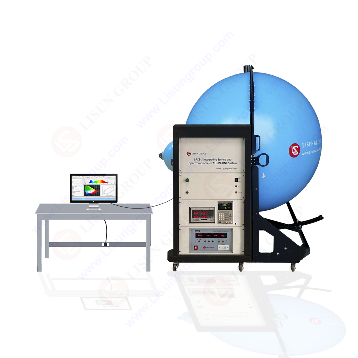


LED luminous efficiency is an important factor to measure photoelectric devices. How to improve the efficiency of LED enables it to achieve the effect of energy saving, this paper has introduced the effective ways of improving LED efficiency from the four aspects including the transparent substrate technology, metal reflecting technology, surface micro structure technology, and flip chip technology.
Transparent substrate technology
InGaAlP LED is usually prepared by InGaAIP luminous zone and Gap window area in the epitaxial growth of GaAs substrate. Compared with InGaAIP, GaAs materials had smaller forbidden band width, therefore, when the light of the short wavelengths injects into GaAs substrate from the luminous zone and window area, it will be fully absorbed and becomes the main reason for the low light device efficiency. There grows a reflecting region between the substrate and restriction layer, which can reflect the light shooting into the substrate in the vertical direction back to luminous zone or window, which has partly improved the LED characteristics of the device. A more effective method is to remove GaAs substrate, replacing the transparent GaP crystal. Because the chip inside has removed the substrate absorption area, which has made the quantum efficiency increase to 25-30% from 4%. Three years ago, to further reduce the absorption of electrode; someone has made this transparent substrate type InGaAlP device into the shape of chamfering cone, and has greatly improved the quantum efficiency. Obviously, this kind of device with the shape of chamfering cone angle has added more light penetration area, in the red light district; the external quantum efficiency of this kind of device is more than 50%.
The relationship of the flux of all kinds of components and the positive current has obviously showed the difference of the three kinds of devices. For the device that absorbs the substrate, because the quantum efficiency is low, the vast majority of input energy has transformed into the hot, under a very small forward current, the LED junction temperature will rise very high, and make the flux ( Flux Meter ) decline rapidly. LED device with transparent substrate, because rather a part of the input power has changed into the luminous energy, which relatively reduces the warming effect, and makes the device work in the much larger current.
Metal reflecting technology
If the transparent substrate process first originated in the U.S.companies such as HP, Lumileds, then a metal reflecting method is mainly used by Japan,Taiwan companies for the research and development. This kind of process not only avoids the transparent substrate patent, but is more advantageous to the scale production. Its effect is the same wonderful as a transparent substrate method. This process is usually called MB process. First remove GaAs underlay, and then steam Al metal film on its surface and Si substrate surface, and then weld them together in a certain temperature and pressure. So, the light emitted from the luminous layer to the substrate layer is reflected by the metal layer to the chip surface, so that the device’s luminous efficiency has improved more than 2.5 times, MB type red LED, when the current is 400 mA and 800 mA, the flux can respectively get to 37lm and 74 lm. Such devices have been put into the small batch production inJapan,Taiwancompanies. Compared with the traditional devices, photosynthetic efficiency has been significantly improved. In addition to the devices with MB structure, the company in Taiwan has also developed a called GB type InGaAlP with high brightness, a new generation of LED devices. The so-called GB is the abbreviation of English Giga Bright. This process has used a new type of scotch tape, which connects the LED epitaxial wafer with GaAs absorbing substrate to sapphire substrates, and then removes away the GaAs absorbing substrate and produces the electrode in epitaxial layer so as to get the high luminous efficiency.
Surface microstructure technology
Surface microstructure technology is an efficient technology to improve the efficiency of the device. The main points in this technology is to sculpture large size on the chip surface as the small structure of the wavelength, each structure shows the shape of chamfering tetrahedron, so it not only expands the luminous area, but also changes the reflecting direction of the light in the chip surface, so that the light efficiency has been improved. Obviously, the existence of the surface texture structure equals a great increase of the thickness of the layer window. The thickness of the window layer is thinner, the corrosion of the texture is deeper, and the increase of light shining rate will be more obvious. For the device with the 20 µm window layer thickness, the light efficiency can increase by 30%. When the window layer thickness decreases to 10 µm, the light efficiency will have a 60% improvement. For the LED device with 585-625 nm wavelengths, after making the texture structure, the luminous efficiency can be up to 30 lm/w, the value has come close to the level of the transparent substrate device.
Flip chip technology
Through the MOCVD technology, GaN LED structure layer grows in the sapphire substrate, the light from the luminous zone of P/N junction shoots out through the above P type area. Because the poor performance of the P type GaN conduction, in order to acquire good current expansion, there needs to form a Ni-Au metal electrodes layer on the P area surface through the steamed plating technology. P area lead through the metal film of this layer draw forth. To obtain good current expansion, Ni-Au metal electrodes layer cannot be too thin. For this reason, the luminous efficiency of the device will be a great influence, which usually includes both the current expansion and the light efficiency. But in any case, the existence of the metal film always makes the light transmitting efficiency become poor. In addition, the existence of the lead solder joints may also affect the light efficiency of the device.
GaN LED backboned chip can fundamentally eliminate the above questions. Because flip-chip is on the Si base pad, the light of LED directly shins out through the sapphire, the above Ni-Au metal film and lead electrodes do not exist. So the light has no losses, in addition to the Ag reflection film on the P-GaN layer, it further boosts the optical intensity of the emergent light. Experiment shows that in 450 ~ 530 nm peak wavelength region, the quantum efficiency of the inversion of the power type LED device is 1.6 times higher than that of ordinary device.
About Lisun Group:
Lead in CFL and LED Tester. Click to our product lists:
Goniophotometer
Spectroradiometer
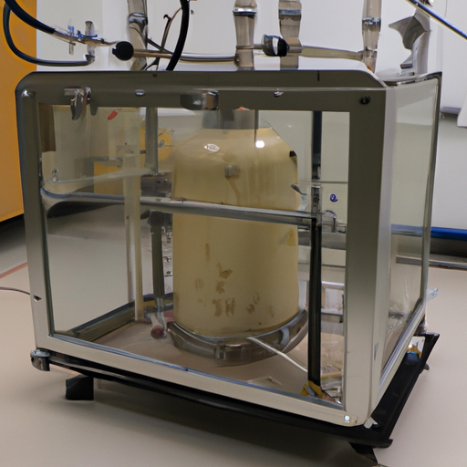
Integrating Sphere
Colorimeter and Photometer
LED Test Instruments
CFL Testing Instruments
EMC testing
Electronic Ballast Tester
Equipments for Testing Electronic components
Electrical Safety Tester
Environmental Chamber
AC and DC power supply
Spectrophotometer