
 中文简体
中文简体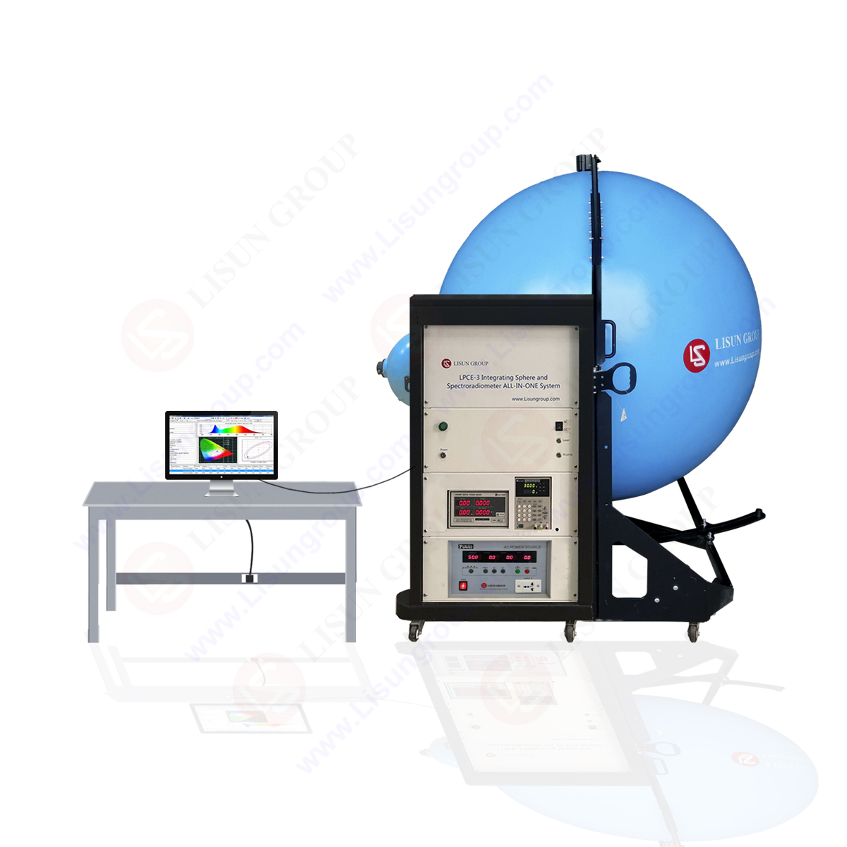


1 Point light source hypothesis
LED is the chip composed of P type semiconductor and N type semiconductor; they have formed the intermediate layer, the PN junction ( LED Junction Temperature ). When p-n junction offsets, electronics and holes will separately inject into PN junction from N type and P type, and is composite and shine. If p-n junction is the square shiny surface, the area is about 0.7mm2 , but LED columnar section area is about 20 mm2 , therefore, p-n junction light-emitting area holds 4%, and we can assume p-n junction light emitting to be as one of the pointillists.
2 Total Reflection Core
When the light is sent out to the optically thinner medium from the optically denser medium and will be totally reflected when the incidence angle is larger than the critical angle. We assume to use the GaAs material with the refractive index of 3.9; the outside packaging materials use the epoxy resin with the refractive index of 1.5. i, =22.60 (we have assumed that p-n junction light emitting is a point light source, therefore, only when i. = 22.6, the photon within a cone can overflow the chip. Shown as figure 2, the reflective photon is assumed not to be sent out because of the internal absorption. In addition, the photon reflected by the p-n junction light source on the lower half plane will also be assumed not to be sent out because of the basement and internal absorption.

Figure 2 total reflection schemes of chip/ epoxy resin interface
3 Hemispheric packaging
In order to protect the semiconductor chip, we usually use the transparent medium to fix it, which is called packaging. Packaging usually uses epoxy resin; the packaging shape directly determines the distribution of light output. As shown in figure 30, we assume that p-n junction luminescence is one light point source 0, the thickness of general LED chip is about 0.5 mm2, we can work out the bilge radius of the circular cone r=0.2 mm by calculating the critical angle, but the radius of the packaging hemisphere is2.5mm, the cone size is 0.8% of it, that can be negligible, therefore, we assume that the light is emitted from the p-n junction luminous point 0. If we adopt the top hemisphere packaging as shown in figure 3, the chip is in the center, we can roughly assume that the light emitted from the chip is perpendicular to the air interface of the epoxy resin, and there is no total reflection. The loss of photon spilled is the reflection loss, it is very convenient to calculate.

Figure 3 hemisphere packaging sketch map
About Lisun Group:
Lead in CFL and LED Tester. Click to our product lists:
Goniophotometer
Spectroradiometer
Integrating Sphere
Colorimeter and Photometer
LED Test Instruments
CFL Testing Instruments
EMC testing
Electronic Ballast Tester
Equipments for Testing Electronic components
Electrical Safety Tester
Environmental Chamber
AC and DC power supply
Spectrophotometer